- 您现在的位置:买卖IC网 > Sheet目录341 > MAX8790AETP+T (Maxim Integrated)IC LED DRVR WHITE BCKLGT 20-TQFN
Six-String White LED Driver with Active
Current Balancing for LCD Panel Applications
Fixed-Frequency Step-Up Controller
The MAX8790A’s fixed-frequency, current-mode, step-
up controller automatically chooses the lowest active
FB_ voltage to regulate the feedback voltage.
Specifically, the difference between the lowest FB_ volt-
age and the current source-control signal plus an offset
(V SAT ) is integrated at the CCV output. The resulting
error signal is compared to the external switch current
plus slope compensation to terminate the switch on-
time. As the load changes, the error amplifier sources
or sinks current to the CCV output to adjust the
required peak inductor current. The slope-compensa-
tion signal is added to the current-sense signal to
improve stability at high duty cycles.
At light loads, the MAX8790A automatically skips pulses
to improve efficiency and prevent overcharging the out-
put capacitor. In SKIP mode, the inductor current ramps
up for a minimum on-time of approximately 150ns, then
discharges the stored energy to the output. The switch
remains off until another pulse is needed to boost the
output voltage.
Internal 5V Linear Regulator
V CC and UVLO
The MAX8790A includes an internal low-dropout linear
regulator (V CC ). When V IN is higher than 5.5V and
SHDN is high, this linear regulator generates a 5V sup-
ply to power an internal PWM controller, control logic,
and MOSFET driver. This linear regulator can deliver at
least 10mA of total additional load current. If V IN is less
than or equal to 5.5V, V CC and IN can be connected
together and powered from an external 5V supply.
There is an internal diode from V CC to IN, so V IN must
be greater than V CC (see Figure 2).
The MAX8790A includes UVLO protection. The controller
is disabled until V CC exceeds the UVLO threshold of
4.25V (typ). Hysteresis on UVLO is approximately 20mV.
The V CC pin should be bypassed to GND with a 1μF or
greater ceramic capacitor.
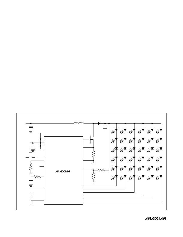
V IN
2.8V TO 5.5V
C IN
L1
0.9 μ H
D1
C OUT
V OUT
UP TO 22V
SHDN
IN
EXT
N1
EXTERNAL
5V SUPPLY
511k Ω
1 μ F
N.C.
V CC
ENA
ISET
BRT
FSET
OSC
CS
GND
R S
30m Ω
R1
1M Ω
OV
1.2k Ω
CCV
MAX8790A
R2
59k Ω
0.1 μ F
FB1
CPLL
0.1 μ F
EP
Figure 3. Low-Input-Voltage Application Circuit
FB2
FB3
FB4
FB5
FB6
12
______________________________________________________________________________________
发布紧急采购,3分钟左右您将得到回复。
相关PDF资料
MAX8790ETP+T
IC LED DRVR WHITE BCKLGT 20-TQFN
MAX8791GTA+
IC MOSFET DRIVER 8-TQFN
MAX8811EEE+
IC DRVR DL PHASE HS 16-QSOP
MAX8821ETI+
IC LED DRVR WHITE BCKLGT 28-TQFN
MAX8822ETE+T
IC LED DRVR WHITE BCKLGT 16-TQFN
MAX8830EWE+T
IC LED DRVR WHITE BCKLGT 16-UCSP
MAX8831EWE+T
IC LED DRIVR WHITE BCKLGT 16-WLP
MAX8834ZEWP+T
IC LED DRIVR BCKLGT FLASH 20-WLP
相关代理商/技术参数
MAX8790AETP+X01
功能描述:LED照明驱动器 Six-String White LED Driver RoHS:否 制造商:STMicroelectronics 输入电压:11.5 V to 23 V 工作频率: 最大电源电流:1.7 mA 输出电流: 最大工作温度: 安装风格:SMD/SMT 封装 / 箱体:SO-16N
MAX8790AEVKIT+
功能描述:LED 照明开发工具 MAX8790A Eval Kit RoHS:否 制造商:Fairchild Semiconductor 产品:Evaluation Kits 用于:FL7732 核心: 电源电压:120V 系列: 封装:
MAX8790ETP+
功能描述:LED照明驱动器 Six-String White LED Driver RoHS:否 制造商:STMicroelectronics 输入电压:11.5 V to 23 V 工作频率: 最大电源电流:1.7 mA 输出电流: 最大工作温度: 安装风格:SMD/SMT 封装 / 箱体:SO-16N
MAX8790ETP+T
功能描述:LED照明驱动器 Six-String White LED Driver RoHS:否 制造商:STMicroelectronics 输入电压:11.5 V to 23 V 工作频率: 最大电源电流:1.7 mA 输出电流: 最大工作温度: 安装风格:SMD/SMT 封装 / 箱体:SO-16N
MAX8790EVKIT+
功能描述:LED 照明开发工具
RoHS:否 制造商:Fairchild Semiconductor 产品:Evaluation Kits 用于:FL7732 核心: 电源电压:120V 系列: 封装:
MAX8791AGTA+
制造商:Rochester Electronics LLC 功能描述: 制造商:Maxim Integrated Products 功能描述:
MAX8791AGTA+T
制造商:Rochester Electronics LLC 功能描述: 制造商:Maxim Integrated Products 功能描述:
MAX8791BGTA+
功能描述:功率驱动器IC Single-Phase Synch MOSFET Driver RoHS:否 制造商:Micrel 产品:MOSFET Gate Drivers 类型:Low Cost High or Low Side MOSFET Driver 上升时间: 下降时间: 电源电压-最大:30 V 电源电压-最小:2.75 V 电源电流: 最大功率耗散: 最大工作温度:+ 85 C 安装风格:SMD/SMT 封装 / 箱体:SOIC-8 封装:Tube
